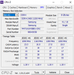
7. Module Type
A = Unbuffered 16-bit Small Outline DIMM (“16b-SO-DIMM”), x16 data bus (placeholder)
B = Unbuffered 32-bit Small Outline DIMM (“32b-SO-DIMM”), x32 data bus (placeholder)
C = Registered 72-bit Small Outline DIMM ("72b-SO-RDIMM”), x64 primary + 8 bit ECC module data bus(placeholder)
E = Unbuffered DIMM ("UDIMM"), x64 primary + 8 bit ECC module data bus
L = Load Reduced DIMM (“LRDIMM”), x64 primary + 8 bit ECC module data bus
N = Mini registered DIMM (“Mini-RDIMM”), x64 primary + 8 bit ECC module data bus
R = Registered DIMM ("RDIMM"), x64 primary + 8 bit ECC module data bus
S = Small Outline DIMM ("SO-DIMM"), no ECC (x64 bit module data bus)
T = Unbuffered 72-bit Small Outline DIMM ("72b-SO-DIMM"), x64 primary + 8 bit ECC module data bus
U = Unbuffered DIMM ("UDIMM"), no ECC (x64 bit module data bus)
W = Mini unbuffered DIMM ("Mini-UDIMM"), x64 primary + 8 bit ECC module data bus
8. Reference design file used for this design (if applicable)
A = Reference design for raw card ’A’ is used for this assembly
B = Reference design for raw card ’B’ is used for this assembly
AC = Reference design for raw card ’AC’ is used for this assembly (example only)
ZZ = None of the JEDEC standard reference designs were used for this assembly
9. Revision number of the reference design used
0 = Initial release
1 = First revision
2 = Second revision
P = Pre-release or Engineering sample
Z = To be used when reference raw card = ZZ
10. JEDEC SPD Revision Encoding and Additions level used on this DIMM